CPU Power Solution with Green-Native Adaptive Voltage Positioning (G-NAVP™)
Topology
Abstract
Along with the evolution of center process unit (CPU), the requirements of
CPU power supply are more and more stringent. However, Richtek has early invested
in CPU power supply development and has proposed numerous CPU power solutions
to meet each CPU power requirements. This application note introduces one of
the Richtek’s patented CPU power solutions, the green-native adaptive voltage
positioning (G-NAVP™) control topology. The G-NAVP™ control topology
features quick response, high efficiency and can meet almost all of the CPU
power specifications. Meanwhile, the G-NAVP™ control is also widely adopted
as nowadays CPU power solution.
1. Introduction of CPU Power Specification
1.1. Microprocessors (Central Processing Unit : CPU)
The microprocessor (central processing unit : CPU) is widely used in many applications
such as computer systems, embedded systems, and handheld devices. In order to
enhance the performance of the microprocessor, more transistors are integrated
in the microprocessor. However, the chip size is reduced due to the improvement
of semiconductor manufacturing technology. The number of integrated transistors
is in accordance with Moore’s Law [1] since the first Intel 4004 microprocessor
was released at 1971. As the Dual-Core Itanium 2 Processor was released in 2006,
the microprocessor has more than a billion transistors and it is about a million
times more than the first Intel 4004 microprocessor [2]. In 2011, Intel introduces
a revolutionary 3-D transistor design called Tri-Gate to improve the performance
and power saving capability [3] which is another milestone of the CPU. However,
the performance of CPU is highly dependent on the voltage regulator (VR) to
balance the input and consumed power. Therefore, Richtek has proposed several
VR controllers to meet the specification of each CPU generation, and the following
will shows the corresponding table.
1.2. Voltage Regulator (VR)
Microprocessors are
becoming increasingly powerful. In other words, the power consumption is dramatically
increasing. In order to satisfy the high current and low voltage power demand
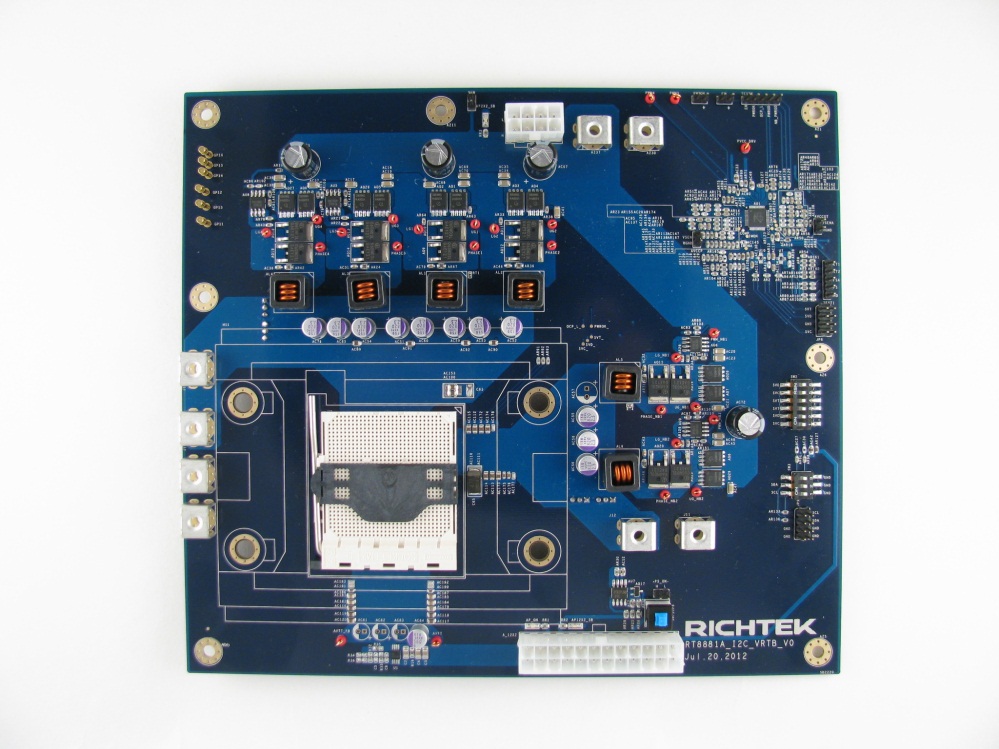
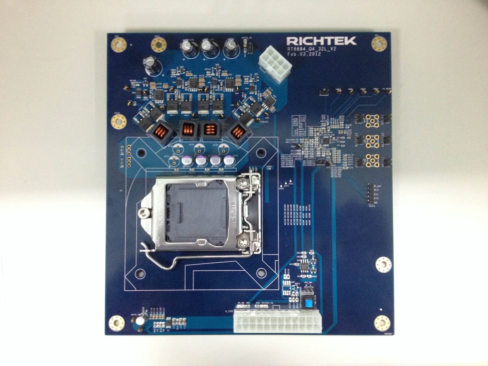
from the microprocessor, the multi-phase voltage regulator (VR) is used. Figure
1 is Richtek’s emulation board for different CPU generation. Figure 1(a) shows
the picture for CPU power solution of AMD SVI2 processor, and Figure 1(b) shows
the picture for CPU power solution of Intel VR12.5 processor.
|
|
|
|
(a)
|
(b)
|
Figure 1. Richtek’s emulation board for different CPU generation.
(a)
AMD SVI2 processor. (b) Intel VR12.5 processor.
Generally speaking, the interleaved multiphase synchronous
Buck converter with voltage-mode control is used in VR. However, today’s VR
faces stringent challenges, not only high current but also strict transient
response requirements. In order to get faster system and reduce the size and
cost, Richtek proposes the G-NAVP™ topology for the multiphase VR. Table
1 to Table 4 shows the corresponding table between Richtek VR controllers and
different CPU power specifications.
Table 1. Richtek VR controller for AMD K8/K8_M2 / Intel
VR10.x & VR11.x CPU Power Solution
|
Controller Part
|
RT8857A
|
RT8862
|
|
Phase Number
|
4/3/2/1 Phase
|
4/3/2/1 Phase
|
|
Integrated Drivers
|
2
|
2
|
|
Control Topology
|
Voltage-Mode
|
Voltage-Mode
|
|
Package
|
WQFN-48L 7x7
|
WQFN-48L 7x7
|
Table 2. Richtek VR controller for Intel VR12 CPU Power
Solution
|
Controller Part
|
RT8859A/M
|
RT8876A
|
|
Phase Number
|
4/3/2/1 + 1 Phase
|
3/2/1 + 1 Phase
|
|
Integrated Drivers
|
0 + 0
|
3 + 0
|
|
Control Topology
|
G-NAVP™
|
G-NAVP™
|
|
Package
|
WQFN-56L 7x7
|
WQFN-56L 7x7
|
Table 3. Richtek VR controller for Intel VR12.5 CPU Power
Solution
|
Controller Part
|
RT8883A
|
RT8889A
|
RT8884A
|
|
Phase Number
|
2/1 Phase
|
3/2/1 Phase
|
4/3/2/1 Phase
|
|
Integrated Drivers
|
2
|
3
|
0
|
|
Control Topology
|
G-NAVP™
|
G-NAVP™
|
G-NAVP™
|
|
Package
|
WQFN-32L 4x4
|
WQFN-40L 5x5
|
WQFN-32L 4x4
|
Table 4. Richtek VR controller for AMD SVI2 CPU Power Solution
|
Controller Part
|
RT8877C/D
|
RT8878A/B
|
RT8881A
|
RT8894A
|
|
Phase Number
|
4/3/2/1 + 2/1/0 Phase
|
4/3/2/1 + 2/1/0 Phase
|
4/3/2/1 + 2/1/0 Phase
|
4/3/2/1 + 2/1/0 Phase
|
|
Integrated Drivers
|
0 + 0
|
2 + 0
|
2 + 0
|
3 + 0
|
|
I2C Interface
|
N/A
|
N/A
|
Support
|
Support
|
|
Control Topology
|
G-NAVP™
|
G-NAVP™
|
G-NAVP™
|
G-NAVP™
|
|
Package
|
WQFN-52L 6x6
|
WQFN-52L 6x6
|
WQFN-52L 6x6
|
WQFN-56L 7x7
|
2. G-NAVP™ Topology Introduction
The G-NAVP™ topology is one type of ripple-based
constant on-time control with current ramp and AVP function. Constant on-time
control features improved light-load efficiency while preserving the heavy-load
efficiency to meet the more and more stringent light-load efficiency specification.
The enhanced light-load efficiency greatly improves the using time of the mobile
productions which is more attractive to the consumers. The AVP function is designed
for the energy and BOM saving purpose, and which is also the feature imposed
by the CPU chip maker such as Intel and AMD.
The abbreviation of G-NAVP™
stands for “Green-native adaptive voltage positioning.” G-NAVP™ topology
provides many attractive features :
- Easy set load-line (droop) for all VR AVP requirements
- Fast transient response which reduces output capacitors and cost
- High efficiency for light load
- High output voltage accuracy for all VR DC requirements
- Ease of use with constant current ripple for all VR ripple requirements
Figure 2 shows the circuit diagram of G-NAVP™ topology.
The G-NAVP™ topology is a constant on-time current-mode control with external
ramp and DC offset cancellation. The error amplifier (EA) is designed to finite
DC gain to adjust the AVP load-line and do the pole and zero compensation. The
current signal is sensed through the DCR current sensing network and modulation
with the external ramp and comp signal. The external ramp is added in the purpose
to increase the noise immunity. The on-time generator will automatic change
the on-time with the input and output voltage to make the inductor current ripple
as constant over the entire input/output range. For more accurate output voltage,
the DC offset cancellation function is added in the loop to cancel the ripple
offset voltage. The functions mentioned above not only increase the robustness
and accuracy of CPU controller but also maintain the good transient response
performance.
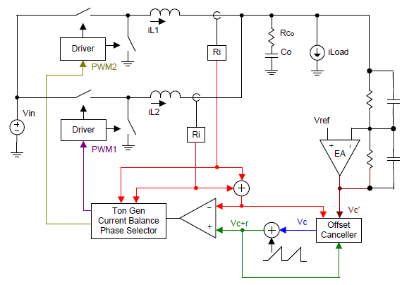
Figure 2. G-NAVP™ control topology circuit diagram.
2.1. Modulation of Constant On-Time Control
Constant on-time control has been widely adopted because
of the faster transient response, good light-load efficiency and smaller component
size. For nowadays mobile products, the longer using time is more attractive
to the consumers. Therefore, the constant on-time control greatly catches designer’s
eye because of the outstanding light-load efficiency.
Constant on-time control
is one of the variable frequency controls. The PWM is modulated by the current
feedback signal and comp signal in the continuous current mode (CCM) as shown
in Figure 3. The control switch turns on when the comp signal touches the current
feedback signal, and turns off after the expiration of the internal one-shot
timer.
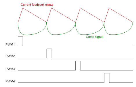
Figure 3. The basic G-NAVP™ modulation behavior waveforms in CCM.
During the load transient period, constant on-time control
automatically changes the switching frequency to speed up the transient response.
For the load step-up transient, the off-time is reduced and equivalent increases
the switching frequency to transfer more energy to the output load as shown
in Figure 4. Moreover, for the load step-down, the off-time is increased to
reduce the switching frequency and ease the overshoot phenomenon.
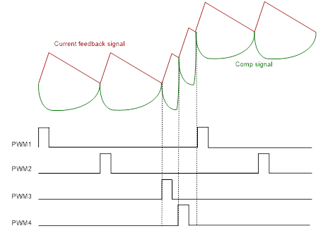
Figure 4. G-NAVP™ modulation behaviors in load step-up condition.
The main benefit of constant on-time control is light-load
efficiency. The switching frequency of the constant on-time control in the discontinuous
current mode (DCM) is proportional to the loading current as shown in Figure
5. At light load, the switching loss is the dominant loss, and the light-load
efficiency can be improved by reduced switching frequency. In Figure 6, we can
see that using constant on-time control at light load condition can achieve
higher efficiency than using constant frequency control.
In DCM operation, the behavior of the low-side MOSFETs
needs to work like a diode, that is, the low-side MOSFETs will turn off when
the inductor current reaches zero. After the low-side MOSFETs are turned off,
the discharge time of output capacitors is dependent with the loading current.
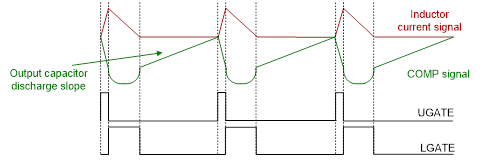
(a) Lighter load condition
Capacitor discharge slope is lower than Figure
5 (b).
(b) Load increased conditionCapacitor discharge slope is higher than Figure
5 (a).
Figure 5. G-NAVP™ control behavior waveforms in DCM.
(a)
Lighter load condition. (b) Load increased condition.
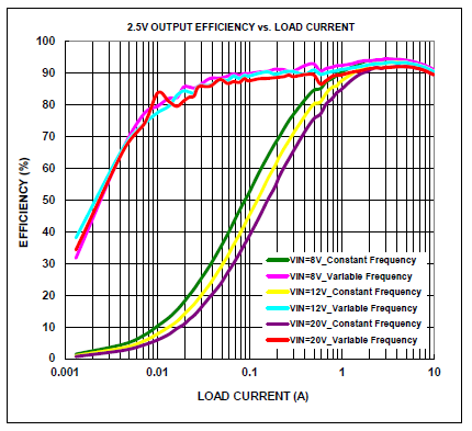
Figure 6. Efficiency comparison between constant frequency control and variable
frequency control.
2.2. Constant Current Ripple
Due to the inductor current ripple is proportional to the
input voltage minus output voltage during the on-time period. The inductor current
ripple may vary with the input voltage and output voltage, and further affect
the output voltage ripple.
 (1)
(1)
The constant current-ripple constant on-time (CCRCOT) mechanism will sense
the input and output voltage and automatically make on-time inverse proportional
to the input and output voltage. With this on-time control methodology, the
G-NAVP™ topology can provide superior output voltage ripple over the wide
input/output operation range to pass the output ripple TOB specification and
can further reduce the output capacitor size.
2.3. Adaptive Voltage Positioning
The design trend of the consuming electronic product becomes smaller and
smaller. However, the size of the power supply is usually dominated by the power
stage component, such as inductors and capacitors. Furthermore, the thermal
issue is more significant when the component size is minimized. In order to
solve the problems above, the adaptive voltage positioning (AVP) function is
proposed for the energy and BOM saving purpose.
The basic idea of AVP is
to control the output voltage level so that it is slightly higher than the minimum
value at full load, and a little lower than the maximum value at light load.
As a result, the entire voltage tolerance window can be used for the voltage
jump or drop during the transient period. Figure 7 shows the transient comparison
between non-AVP and AVP designs [4]-[5]. Therefore, the AVP design allows customers
to use fewer output capacitors to reduce the VR cost. Besides, the AVP control
greatly facilitates the thermal design because the VR output power at full load
is degraded.
To implement the AVP function, the VR output impedance needs
to be designed as constant as shown in Figure 8.
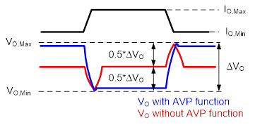
Figure 7. The behavior of AVP function.
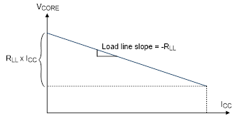
Figure 8. The relation between loading current and output voltage.
Instead of using complicated type-3 compensator, the G-NAVP™
topology adopts a low gain compensator (one pole and one zero) and further utilize
the steady-state error, which is the native of low gain compensation, to do
the AVP function. For this reason, this control topology is called as native
adaptive voltage position (NAVP).
In the G-NAVP™ topology, the AVP
function is achieved by set the load line (droop) via the current loop and the
voltage loop. For user friendly purpose, Richtek provides a brief load line
setting equation in corresponding specific IC datasheet.
2.4. Ramp Compensation
Considering the noise margin and jitter, the G-NAVP™
topology adopts a ramp compensation to increase noise immunity and reduce jitter
at the switching node. Besides, with appropriate design, the ramp compensation
can also smooth the mode transient behaviors. Figure 9 shows the noise margin
with and without ramp compensation.
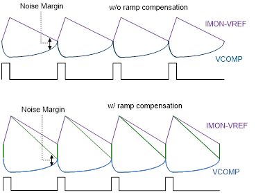
Figure 9. The noise margin with and without ramp compensation.
3. Conclusion
Along with the growth of the mobile productions, the efficiency
catches more attentions due to the finite battery time and thermal consideration.
To satisfy both the performance and efficiency requirements, Richtek provides
the G-NAVP™ topology to fulfill the consumer’s requirements.
The G-NAVP™ topology adopts ripple-based constant
on-time control with current ramp and AVP function. Constant on-time control
features quick response and high efficiency, and the AVP function provides good
BOM saving capability. The offset cancellation circuit and the ramp compensation
increase the DC accuracy and noise immunity. Combine with the above functions,
the G-NAVP™ is an outstanding VR controller and can meet almost all of
the VR power specification from Intel and AMD applications.
4. Reference
|
[1]
|
Intel document, “Moore’s Law Timeline,” Available
at
http://download.intel.com/pressroom/kits/events/moores_law_40th/MLTimeline.pdf
|
|
[2]
|
Intel document, “Intel Processor History,”
Available at
http://download.intel.com/pressroom/kits/IntelProcessorHistory.pdf
|
|
[3]
|
Intel document, “Intel®’s 22nm Technologys
Moves Transistor Into the 3rd Dimension,” Available at
http://www.intel.com/content/dam/www/public/us/en/documents/backgrounders/standards-22-nanometers-technology-backgrounder.pdf
|
|
[4]
|
Kaiwei Yao, Yuancheng Ren, Julu Sun, Kisun
Lee, Ming Xu, Jinghai Zhou and Fred C. Lee, “Adaptive Voltage Position
Design for Voltage Regulators,” IEEE APEC’04.
|
|
[5]
|
Jian Rong Huang, Sophia Chien-Hui Wang, Chia
Jung Lee, Eddie Kuo-Lung Tseng and Dan Chen, “Native AVP Control
Method for Constant Output Impedance of DC Power Converters,” IEEE
PESC’07.
|